


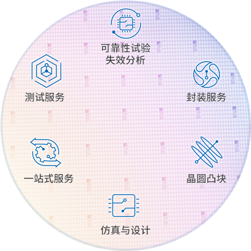


Technical Highlights
Advancement of Mainstream Package

Patented HFBP technology for power and signal chain products, with over 10 billion shipments

ECP fan-in and fan-out WLP provides ultra-thin six-sided protection; Full-process capability for power devices with backside metal and frontside copper-nickel-gold RDL

Wide-body SOIC / TSSOP and internal insulation solutions for high-voltage isolation applications

Packaging structures and processes for a full range of sensors including pressure, inertial, magnetic, and optical


&e6&a8&a1&e5&9d&97.png)


