


The “Invisible Engine” Behind Smartphones: JCET’s RFFE Packaging Technology Elevates User Experience
Company News
2025-09-11
Share:


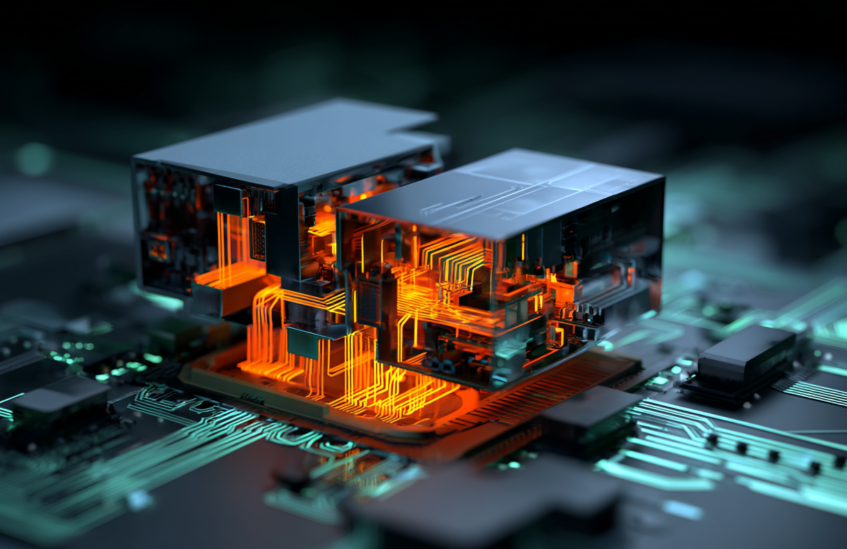
The radio frequency front-end module (RFFEM) serves as the “core engine” driving smartphones’ communication capabilities. Responsible for transmitting, receiving, processing, and optimizing signals, it is one of the most vital components in modern mobile devices. In next-generation high-end smartphones, powerful chips provide the hardware foundation for intelligent applications to seamlessly integrate into everyday life. Enhancing this foundation, the RFFE module utilizes fully integrated designs, advanced materials, and system-level packaging innovations to meet the demands of the smart era and deliver superior user experiences.
As a leading provider of semiconductor packaging and testing services, JCET offers comprehensive RF packaging and testing solutions. The company has built deep expertise and production capacity in high-density DsmBGA, 3D SiP, cavity shielding, and antenna-in-package (AiP) technologies. These capabilities support global customers in upgrading their 5G and Wi-Fi RF modules, as well as millimeter-wave radar products.
Located between a smartphone’s antenna and baseband chip, the RFFE module integrates transmission and reception chains with duplexers and multiplexers, enabling simultaneous signal processing. Through dynamic tuning, it helps reduce power consumption and extend battery life. In high-end smartphones, RFFE modules feature highly customized solutions that combine power amplifiers, switches, and filters into a single compact module. Embedded shielding layers within the module help minimize chip-to-chip interference.
With nearly two decades of experience in system-in-package (SiP) technology, JCET has developed high-density heterogeneous integration SiP solutions tailored for next-generation smartphone RF modules. These solutions offer high integration, excellent yield, and the ability to combine diverse components—such as filters, power amplifiers, and switches—into a single package, meeting the complex demands of 5G multi-band systems. JCET’s dual-side SiP packaging technology supports placement accuracy up to 15 microns and components as small as 008004, significantly reducing module size.
JCET also employs sputtering-based shielding techniques to achieve cavity or selective electromagnetic shielding, effectively minimizing signal interference. Its cavity protection solutions enable bare-die packaging for filters, enhancing high-frequency stability while lowering packaging costs. Additionally, JCET has established comprehensive validation and testing platforms covering RF microwave, millimeter-wave, 5G cellular, and wireless communications. These platforms support end-to-end validation—from chips and packaging to modules and final products—ensuring product reliability and performance.
“JCET’s advanced high-density SiP integration technologies and mass-production expertise have enabled robust global delivery capabilities for high-end RF module packaging and testing,” said Owen Jin, Vice President of JCET and General Manager of the AI & Smart Applications Business Unit. “Our technologies span the entire process—from design to testing—and will continue to deliver high-performance, miniaturized, and highly reliable RF solutions for smart devices, automotive electronics, and satellite communications, ultimately enhancing the intelligent experience for end users.”