
 English
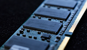
Semiconductor companies are continually faced with complex integration challenges as consumers want their electronics to be smaller, faster, and higher performance with more and more functionality packed into a single device. Semiconductor packaging has a significant impact on addressing these challenges. Current and future demands for greater system performance, increased functionality, reduced power consumption, and reduced form factor require an advanced packaging approach known as system integration.
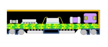
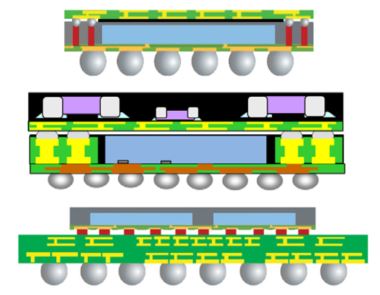
System integration is combining multiple integrated circuits (ICs) and components into a single system or modularized sub-system in order to achieve higher performance, functionality, and processing speeds with a significant reduction in space requirements inside the electronics device.
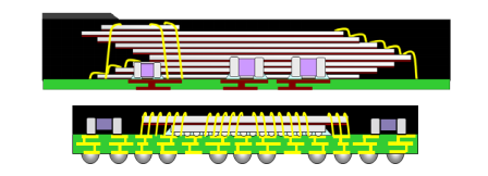
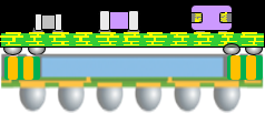
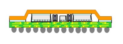
JCET SiP solutions are enhanced by multiple advanced technologies including double-sided molding technology, EMI electromagnetic shielding technology, and laser-assisted bonding (LAB).
1. Double-sided molding: the technology effectively reduces the package size, shortens the connection of multiple dies and passive devices, reduces resistance, and improves the electrical performance of the system.
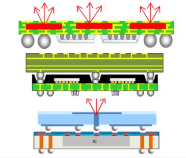
2. EMI shielding: JCET uses back metallization technology to effectively improve thermal conductivity and EMI shielding.
3. Laser-assisted bonding (LAB): the technology is able to overcome traditional reflow bonding problems, such as CTE mismatch, high warpage, high thermal mechanical stress, and other reliability problems.
Applications


Download Documents


