 English
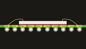
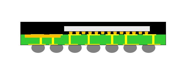
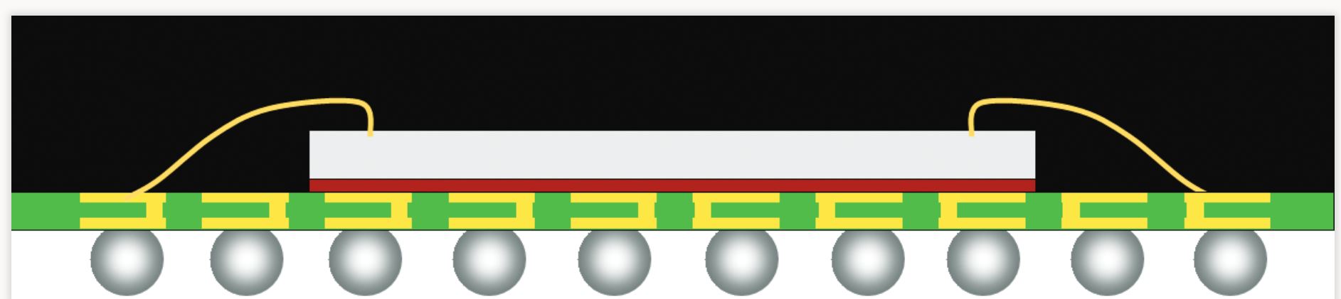
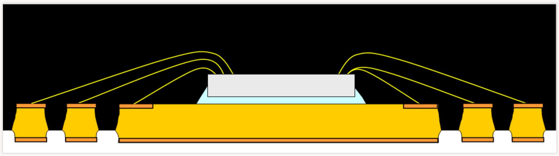
In the 5G era, high-frequency, high-speed, low-latency, and multi-channel characteristics have brought new technical challenges to integrated circuit packaging. JCET provides a full range of advanced packaging and testing solutions, including 2.5D/3D packaging, wafer-level packaging, system-in-package (SiP), etc., and one-stop solutions, including collaborative design/simulation, selection of high-density integration processes, and the use of automated processes to ensure product quality. In terms of high-density packaging and integration technology, JCET provides a number of industry-leading technologies including high-density mounting SMT capability, laser-assisted bonding (LAB), double-sided molding SiP, electromagnetic interference shielding, etc., which can be used in RF front-end modules (RFFE), millimeter-wave antenna AiP module and other products.
 Baseband
 RF
RF Infrastructure
Our Advantages
RF Co-Design & Simulation
High-Speed EMI Shielding
RFFE SiP & 5G AiP Toolbox
Low-Dk/Df BOM Selection
Turnkey 5G Testing Service

More Applications