
 English
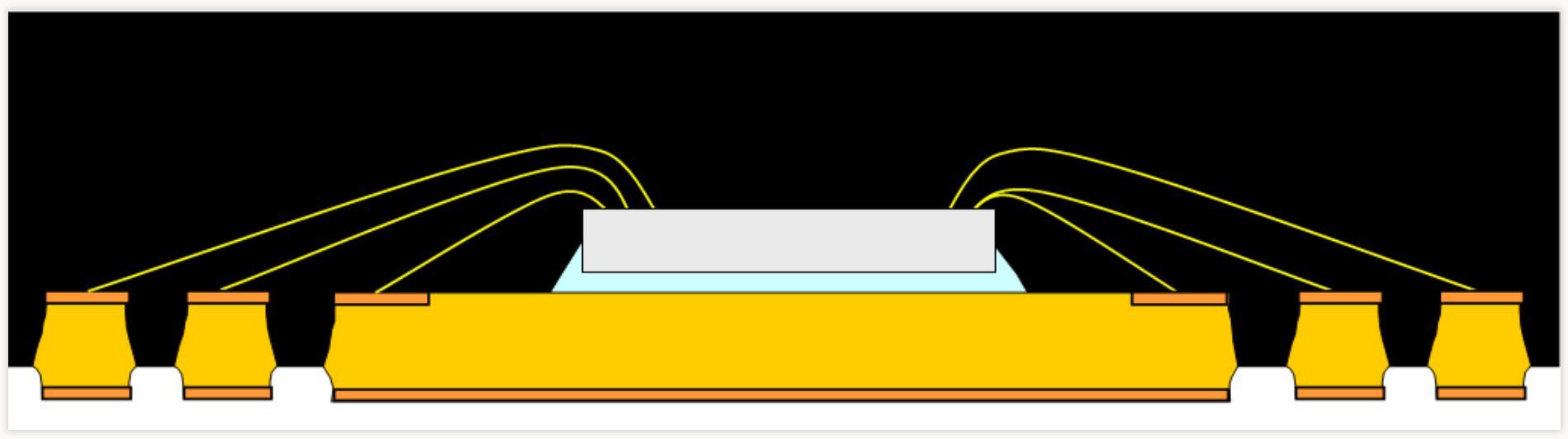
Wire bonding forms an interconnection between a chip to a substrate, substrate to substrate, or substrate to a package. Wire bonding is generally considered the most cost-effective and flexible interconnect technology, and is used to assemble the vast majority of semiconductor packages today.
Wire Bond interconnection is available in a number of packaging approaches at JCET, including gold wire, silver alloy wire, copper wire, aluminum wire, and aluminum tape. As a low-cost alternative to gold wire, copper wire is becoming the preferred interconnect material in wire bond packaging. Copper wires have similar electrical characteristics and performance to gold wires, and have lower resistance. This is a big advantage when lower wire bonding resistance is required to improve device performance.
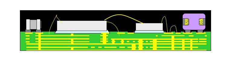
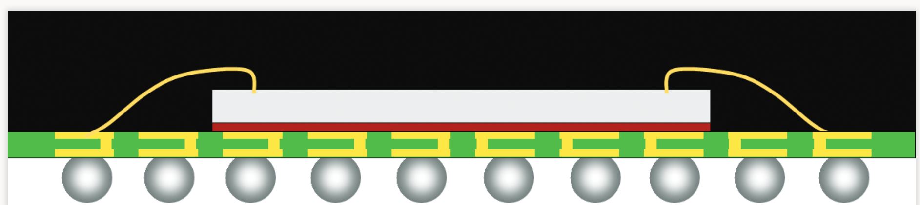
Laminate-based Ball Grid Array interconnect technology(BGA) was first introduce as a solution to the increasingly high lead counts required for advanced semiconductors. BGA technology features leads on the bottom surface of the package in the form of small bumps or solder balls, and provides low inductance, ease of surface mounting, relatively low cost, and excellent package reliability. JCET offers a full suite of laminate-based BGA packages, including fine pitch, extremely thin, multi-die, stacked, and thermally enhanced configurations.
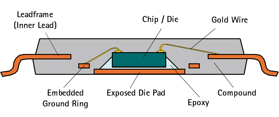
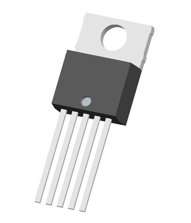
Leaded packages are characterized by a die encapsulated in a plastic mold compound with metal leas surrounding the perimeter of the package. this simple and low-cost packaging is still the best solution for many applications. JCET provides a comprehensive range of leadframe package solutions from standard leadframe packages to low profile, small and thin, thermally enhanced packages, including Quad Flat Package(QFP), Quad/Dual Flat No-lead package(QFN/DFN), and Thin Small Outline Packages(TSOP), Small Outline Transistors(SOT), Small Outline Packages (SOP), Dual Inline Packages (DIP), Transistor Outline (TO).
Technology Solutions


Download Documents
- FLGA - Fine Pitch Land Grid ArrayLQFP - Low Profile Quad Flat Pack
- LQFP-ep - Enhanced Low Profile Quad Flat Pack
- MQFP - Metric Quad Flat Pack
- PBGA - Plastic Ball Grid Array
- PBGA-H - Plastic Ball Grid Array with Heat Spreader
- PBGA-MD - Plastic Ball Grid Array with Multi-Die
- QFN - Quad Flat No-Lead Package (punched and saw singulated versions)
- QFNs-st - Quad Flat No-Lead Package (Stand-off Terminal)
- TQFP - Thin Profile Quad Flat Pack
- TQFP-ep - Enhanced Thin Profile Quad Flat Pack
- FBGA - Fine Pitch Ball Grid Array
- FLGA - Fine Pitch Land Grid Array


