
 English
The market for portable and mobile data access devices is growing rapidly, driving the demand for both increased functional convergence as well as increased packaging complexity and sophistication. Accelerated by the need for higher levels of integration, improved electrical performance, or reduction of timing delays, the requirements for shorter vertical interconnects are forcing a shift in packaging technology from 2D packaging to more advanced 2.5D and 3D package designs. To meet this demand, various types of stacking integration technologies are being used to combine multiple chips with diverse functionality into increasingly smaller and smaller sizes.
JCET has been actively pushing the boundaries of traditional packaging paradigms by pioneering a number of enabling integration technologies in wafer level packaging, flip chip interconnect, and Through Silicon Via (TSV) to develop differentiated solutions that position its customers for success in the markets they serve.
Applications

Download Documents
- Bare Die fcPoP - Flip Chip Package-on-Package
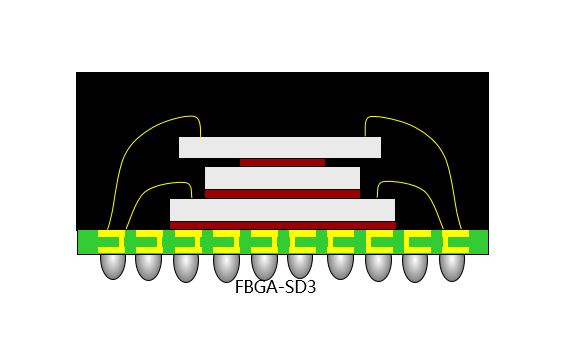
- FBGA-SD - Fine-Pitch Ball Grid Array with Stacked Die
- Fi-PoP - Fan-in Package-on-Package
- Molded Laser fcPoP - Flip Chip Package-on-Package
- PBGA-SD - Plastic Ball Grid Array with Stacked Die
- PiP - Package-in-Package
- PoP - Package-on-Package
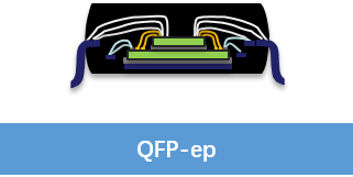
- QFP-SD - Quad Flat Pack with Stacked Die
- TSOP-SD - Thin Small Outline Package with Stacked Die


